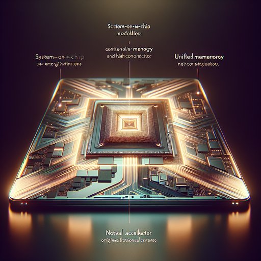
Motherboards have transformed from simple interconnects into high-speed, high-power platforms that orchestrate dozens of standards without compromising stability. The push for PCIe 5.0 bandwidth, multi-hundred–ampere CPU transients, and a tangle of modern I/O—USB4, Thunderbolt, NVMe, Wi‑Fi, and legacy interfaces—has forced sweeping changes in board layout, materials, firmware, and validation. What used to be a question of slot count is now a careful exercise in signal integrity budgeting, power delivery engineering, and standards negotiation. Understanding how motherboards evolved to meet these demands reveals the quiet, meticulous work that enables today’s CPUs, GPUs, and SSDs to reach their potential while still welcoming older devices.
The modern motherboard’s relevance stems from its role as the convergence point for ever-faster compute, storage, and peripheral technologies. As processors added cores and accelerators, and as GPUs and SSDs demanded more lanes and lower latency, the board became a system-level engineering challenge rather than a passive backplane. Designers had to deliver clean power at high currents, route multi-gigahertz signals across complex stacks of copper, and maintain compatibility with components spanning decades of standards. This evolution tracks the broader history of computing: more performance per watt, more integration per square centimeter, and tighter coordination between silicon, firmware, and layout.
Raising PCIe to 5.0 speeds pushed motherboard construction into techniques once reserved for networking gear and servers. Instead of four-layer boards with generous trace runs, many enthusiast and workstation designs moved to 8–12 layers, heavier copper, and back-drilled vias to eliminate signal-degrading stubs. Controlled-impedance routing, continuous reference planes, and careful layer ordering became mandatory to keep insertion loss within the channel budget. Even connector choice and slot reinforcement mattered, because mechanical deflection and discontinuities can shift impedance and erode margin at 32 gigatransfers per second.
PCIe 5.0 retains 128b/130b encoding and doubles per-lane rate to 32 GT/s, but achieving that on a desktop board often requires redrivers or retimers when trace lengths or topologies exceed the allowed loss. Vendors frequently bifurcate the CPU’s x16 graphics link into x8/x8 or x8 plus one or two M.2 sockets, balancing flexibility against signal integrity and lane availability. Some boards route a PCIe 5.0 x4 link to an M.2 slot for next-generation NVMe SSDs, with dedicated heatsinks and short traces to avoid retimers. Backward compatibility remains intact, so older PCIe cards train down seamlessly, but designers still budget for crosstalk, skew, and equalization across every lane.
Power delivery changed just as dramatically. Today’s desktop CPUs can draw sustained currents well above 200 A with fast transient edges, so VRMs employ cascaded multiphase controllers, smart power stages, and low-DCR chokes sized for low ripple and quick response. Load-line definitions from modern voltage specifications, along with high switching frequencies and doubled-up phases, help meet transient targets without overshoot. The shift to EPS12V 8-pin connectors, sometimes in pairs, gives headroom for peak loads at reasonable cable temperatures.
Meanwhile, the ATX12VO initiative moves 3.3 V and 5 V conversion onto the motherboard, simplifying power supplies and improving idle efficiency at the cost of greater board-level regulation and thermal design. Memory standards added another layer of complexity in both hardware and firmware. DDR5 relocates key power management to a PMIC on the DIMM, so the motherboard must deliver a clean 5 V feed and accommodate new signal training behaviors and topologies. Early platforms offered separate DDR4 and DDR5 board variants for the same CPU socket because routing constraints, termination strategies, and layer budgets differ meaningfully between the standards.
Motherboards implement fly-by topologies, tight length matching, and careful stub minimization, then rely on UEFI firmware to train timings across DIMM types, ranks, and capacities. On-die ECC in DDR5 improves chip-level reliability but does not replace end-to-end ECC; boards that support ECC still require appropriate CPUs and modules. I/O integration widened the scope from lanes and slots to entire subsystems. USB 3.2 at 20 Gbps demands short, well-shielded paths and sometimes re-timers for front-panel connectors; USB4 and Thunderbolt 4 typically add dedicated controllers plus DisplayPort routing for alt-mode.
Delivering reliable USB-C power requires PD controllers and robust protection circuits, all while meeting electromagnetic compatibility limits. NVMe via M.2 comes in multiple key types, with Wi‑Fi and Bluetooth often on E-key sockets that may depend on platform-specific interfaces. Chipset links carry enormous traffic: recent Intel platforms use a DMI 4.0 x8 link comparable to PCIe 4.0 x8, while many AMD AM5 implementations connect the CPU to the chipset over PCIe 4.0 x4, with the CPU providing PCIe 5.0 lanes directly to graphics and storage. The invisible glue is firmware and system management.
UEFI replaced legacy BIOS to support NVMe boot, Secure Boot, flexible PCIe bifurcation, and capsule updates that can be deployed by operating systems. Platform security modules are now commonly integrated as firmware TPMs in the chipset or CPU, meeting modern OS requirements without a discrete chip. Memory training algorithms and voltage regulators are coordinated by embedded controllers that monitor temperature sensors and adjust fans, ensuring signal integrity and power delivery remain within spec under changing workloads. Features like safe-recovery flash utilities and dual-ROM designs reduce the risk inherent in field updates on increasingly complex boards.
All of this integration occurs under the constraint of compatibility with older devices and cases. Motherboards still expose SATA ports, legacy USB, and sometimes serial headers, while juggling lane sharing between M.2 slots and SATA controllers to avoid user surprises. Mechanical form factors such as ATX, microATX, and Mini-ITX have endured, but board makers reinforce PCIe slots, add backplates, and route front-panel USB-C headers to match modern cases. Validation efforts now include exhaustive device matrices, thermal and acoustic profiling for M.2 and VRMs, and interoperability testing for USB4 and DisplayPort alt-mode.
The result is a platform that feels simple to assemble yet hides a stack of engineering trade-offs. Looking ahead, the same forces will intensify. PCIe 6.0 doubles bandwidth again using PAM4 signaling and forward error correction, shrinking link margins and increasing reliance on retimers, tighter materials control, and meticulous connector design. DDR5 speeds will climb, placing more pressure on trace topology and firmware training, while ATX12VO and similar efficiency initiatives may spread beyond OEM systems.
As accelerators, high-speed storage, and external displays proliferate, the board will continue mediating between diverse standards and physical constraints. The motherboard’s evolution shows how careful platform engineering unlocks silicon advances—and how it will remain pivotal as computing demands grow.